
PCB Design Workshop • Indore

PCB Design Workshop in Indore

Design • Build • Test your own PCB.

A practical, industry-oriented workshop by Genixotech that gives participants the confidence to design schematics, create PCB layouts, generate manufacturing files, assemble components and safely test their own boards — no prior PCB design experience needed.

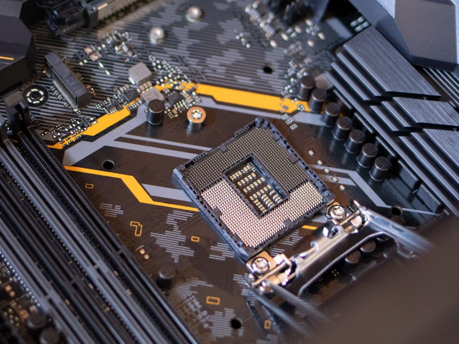
Close-up of a printed circuit board with a processor socket
  • 2 Days16 learning hours
  • Mini ProjectYour own PCB
  • CertificateOf completion
Duration2 Days • 16 Learning Hours
Methodology100% Practical & Project-Based
Final outputManufacturing-Ready PCB Package

Why choose Genixotech

Built for practical confidence.

Complete design-to-manufacturing workflow
KiCad-first practical training
Real schematic and layout exercises
Gerber and BOM generation
Soldering and assembly practice
Multimeter-based PCB testing
Industry-oriented design rules
Independent final mini project

This workshop does not promise overnight expertise. It builds a reliable foundation and guides every participant through the full design-to-testing workflow using practical exercises and an independent mini project.

Workshop curriculum

Two days from fundamentals to a manufacturing-ready PCB.

Each day maps structured theory to live laboratory hardware set-ups.

Module01

Introduction to PCB Technology45 min

Topics covered

  • What a PCB is and why it matters
  • PCB vs. breadboard and common applications
  • Overview of the PCB manufacturing process
  • Single, double and multilayer PCBs
  • Flex, rigid, rigid-flex and metal-core PCBs
Module02

PCB Components, Packages & Footprints45 min

Topics covered

  • Through-hole and SMD components
  • DIP, SOIC, TQFP, QFN and BGA introduction
  • Reading component datasheets
  • Understanding symbols vs. footprints
Module03

Industry PCB Design Flow45 min

Topics covered

  • Idea and circuit design
  • Schematic and component selection
  • Footprint assignment and PCB layout
  • DRC, Gerber, manufacturing, assembly and testing
Module04

Introduction to KiCad / EasyEDA1 hour

Topics covered

  • Installation and interface orientation
  • Projects, libraries and preferences
  • Essential shortcuts
  • Practical library management
Module05

Schematic Design2 hours

Topics covered

  • Create a project and add components
  • Power symbols, ground and net labels
  • Annotation, ERC and schematic best practices
  • Generate a Bill of Materials (BOM)

Hands-on session

  • LED Blinker or 555 Timer Circuit
Module06

PCB Layout Basics2 hours

Topics covered

  • Board outline and component placement
  • Manual vs. automatic routing
  • Track width, clearance and copper pour
  • Ground plane, silkscreen and reference designators
  • Mounting holes and layout review

Hands-on session

  • Create Your First PCB

Technologies, tools & frameworks covered

Primary softwareKiCad
Optional softwareEasyEDA
BringLaptop with KiCad
TestMultimeter
SolderSoldering Station
ConsumablesFlux & Solder Wire
ReworkDesoldering Pump / Wick
Hand toolsTweezers & Side Cutter
InspectionMagnifying Glass
PartsPrototype Components

Hands-on projects

Choose your mini project.

Participants select a project based on their current electronics experience, from a simple LED flasher to an STM32 breakout board.

Book this workshop
  1. 01LED Flasher Beginner
  2. 02Power Supply Board Beginner
  3. 03Traffic Light Circuit Beginner
  4. 04Arduino Shield Intermediate
  5. 05Relay Driver Board Intermediate
  6. 06IR Sensor Board Intermediate
  7. 07ESP32 Development Board Advanced
  8. 08ATmega328P Minimum System Advanced
  9. 09STM32 Breakout Board Advanced

Learning outcomes

After the workshop, students will be able to:

  • Understand the complete PCB design lifecycle
  • Read datasheets and select appropriate footprints
  • Create clear, professional electronic schematics
  • Design single- and simple double-layer PCBs
  • Apply routing and design-rule best practices
  • Generate manufacturing-ready Gerber and drill files
  • Assemble and test basic PCBs safely
  • Order fabricated PCBs from manufacturers

Get certified upon completion.

Leave with complete design files, a manufacturing package, practical assembly experience and a verified Genixotech Certificate of Completion to share on LinkedIn and your CV.

  • Shareable on LinkedIn profiles & technical CVs
  • Validated credential with signature reference

Get in touch

Book your seat in the PCB Design Workshop.

Tell us your department, student strength and preferred dates. We will send a workshop proposal with format, kit and schedule details.

For colleges & institutions

Request a workshop proposal

For Directors, Deans, TPOs, HODs and college management. Fields marked * are required.

Ready to design your first PCB?

Start with a one-day workshop or run the full three-day advanced program.